ISSI DDR SDRAM
ISSI 512-Mbit DDR SDRAM achieves high-speed data transfer using pipeline architecture and two data word accesses per clock cycle. The 536,870,912-bit memory array is internally organized as four banks of 128Mb to allow concurrent operations. The pipeline allows Read and Write burst accesses to be virtually continuous, with the option to concatenate or truncate the bursts. The programmable features of burst length, burst sequence, and CAS latency enable further advantages. The device is available in 8-bit, 16-bit, and 32-bit data word sizes. Input data is registered on the I/O pins on both edges of Data Strobe signal(s), while output data is referenced to both edges of Data Strobe and both edges of CLK. ISSI 512-Mbit DDR SDRAM commands are registered on the positive edges of CLK.Features
- VDD and VDDQ: 2.5V ± 0.2V (-6)
- VDD and VDDQ: 2.6V ± 0.1V (-5)
- SSTL_2 compatible I/O
- Double-data rate architecture
- Bidirectional, data strobe (DQS) is transmitted/received with data, to be used in capturing data at the receiver
- DQS is edge-aligned with data for READs and centre-aligned with data for WRITEs
- Differential clock inputs (CK and CK)
- DLL aligns DQ and DQS transitions with CK transitions
- Commands entered on each positive CK edge
- Four internal banks for concurrent operation
- Data mask for write data
- 2, 4, and 8 burst lengths
- Sequential and interleave mode burst type
- 2, 2.5, and 3 programmable CAS latency
- Auto refresh and self refresh modes
- Auto precharge
- TRAS Lockout supported (tRAP = tRCD)
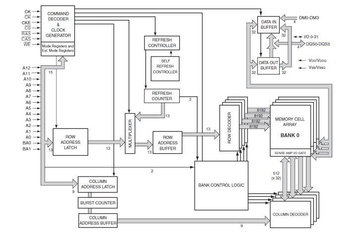
Functional Block Diagram

게시일: 2014-08-21
| 갱신일: 2025-08-07


