


Texas Instruments Texas Instruments DAC3482EVM 평가 모듈(EVM)
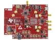
Texas Instruments DAC3482EVM 평가 모듈(EVM)은 설계자가 TI의 2채널 초저전력 16비트 1.25GSPS DAC3482 디지털 아날로그 변환기(DAC)를 평가하기 위한 용도로 사용되는 회로 보드이며, DAC3482 디지털 아날로그 변환기는 16비트 및 8비트 폭의 DDR LVDS 데이터 입력, 통합 2x/4x/8x/16x 인터폴레이션 필터, 32비트 NCO 및 PLL, 고역 IF에서의 뛰어난 선형성이 특징입니다. 이 평가 모듈은 다양한 클럭과 데이터 입력 및 IF 출력 조건에서 DAC3482를 시험하기 위한 유연한 환경을 제공합니다. 완전한 IF 송신기 솔루션으로서의 간편한 사용을 위해, DAC3482EVM에는 CDCE62005 클럭 생성기/지터 제거기가 내장되어 DAC3482에 대한 클러킹을 수행합니다 . DAC3482에 고품질 저지터 DAC 샘플링 클럭을 제공하는 것 외에도, CDCE62005는 또한 TSW1400EVM(또는 TSW3100EVM)에 FPGA 기준 클럭으로서 FPGA 클럭을 제공합니다.
특징
- Superior performance
- 550fs rms typical low noise clock generator (10kHz to 20MHz integration bandwidth), FC = 100MHz
- 2.6ps rms typical low noise jitter cleaner (10kHz to 20MHz integration bandwidth), FC = 100MHz
- Flexible frequency planning
- 5x fully configurable outputs: LVPECL, LVDS, LVCMOS, and special high swing output modes
- Unique dual-VCO architecture supports a wide 1.750GHz to 2.356GHz tuning range
- Output frequency ranges
- 4.25MHz to 1.175GHz in synthesizer mode
- Up to 1.5GHz in fan-out mode
- Independent coarse skew control on all outputs
- High flexibility
- Integrated EEPROM determines device configuration at power-up
- Smart input multiplexer automatically switches between one of three reference inputs
- 7mm × 7mm, 48-pin VQFN package (RGZ)
- -40°C to +85°C temperature range
애플리케이션
- Wireless infrastructure
- Switches and routers
- Medical electronics
- Military and aerospace
- Industrial
사양
- -0.5V to 4.6V supply voltage range
- ±20mA input current
- ESD ratings
- 2000V maximum human body model
- 750V maximum charged device model
- ±50mA output current for LVPECL/LVCMOS outputs
- 3pF input capacitance
- 50Ω ESR
- 10-year data retention
Functional Block Diagram
")
Related Development Tools

Texas Instruments Texas Instruments CDCE62005EVM 평가 모듈(EVM)
고성능 저위상잡음 주파수 합성기 겸 지터 제거기인 CDCE62005를 평가하기 위한 용도입니다.

Texas Instruments DAC34SH84EVM Evaluation Module (EVM)
Allows designers to evaluate the performance of TI's DAC34SH84 digital-to-analog converter (DAC).
Texas Instruments Texas Instruments DAC3283EVM 평가 모듈(EVM)
TI의 이중 채널 16비트 800MSPS DAC3283 디지털 아날로그 변환기를 평가합니다.

Texas Instruments Texas Instruments DAC3484EVM 평가 모듈(EVM)
TI의 4채널 초저전력 16비트 1.25GSPS DAC3484 디지털 아날로그 변환기를 평가하기 위한 용도로 사용됩니다.
Texas Instruments Texas Instruments DAC3484EVM 평가 모듈(EVM)
TI의 4채널 초저전력 16비트 1.25GSPS DAC3484 디지털 아날로그 변환기를 평가하기 위한 용도로 사용됩니다.

Texas Instruments Texas Instruments DAC34H84EVM 평가 모듈(EVM)
TI의 4채널 초저전력 16비트 1.25GSPS DAC34H84 디지털 아날로그 변환기를 평가하기 위한 용도로 사용됩니다.
게시일: 2016-01-19
| 갱신일: 2022-03-11