


Infineon Technologies PSoC®4XX8_BLE 임베디드 시스템 컨트롤러
Cypress Semiconductor PSoC® 4XX8_BLE 임베디드 시스템 컨트롤러는 임베디드시스템 컨트롤러를 위한 확장가능하고 구성가능한 플랫폼을 제공합니다. 이 컨트롤러에는 프로그래밍 가능하며 재구성 가능한 아날로그 및 디지털 블록과 유연한 자동 라우팅 기능이 결합된 ARM®Cortex™-M0 CPU가 탑재되어 있습니다. PSoC 4XX8_BLE는 마이크로컨트롤러를 통합형 Bluetooth 저에너지(BLE)와 결합한 솔루션으로 Bluetooth Smart, 무선 장치 및 서브시스템(BLESS)이라고도 부릅니다. 포함된 기능으로는 디지털 프로그래밍 가능 로직, 고성능, 아날로그-디지털 컨버터(ADC), 연산 증폭기가 있습니다. PSoC 4XX8_BLE 제품은 새로운 애플리케이션 및 설계 조건에서 PSoC4 플랫폼 요소와 호환됩니다.
특징
- 32-bit MCU subsystem
- 48MHz Arm Cortex-M0 CPU with single-cycle multiply
- Up to 256KB of flash with read accelerator
- Up to 32KB of SRAM
- BLE radio and subsystem
- 2.4GHz RF transceiver with 50Ω antenna drive
- Digital PHY
- Link-layer engine supporting master and slave modes
- RF output power: -18dBm to +3dBm
- RX sensitivity: -92dBm
- RX current: 18.7mA
- TX current: 16.5mA at 0dBm
- RSSI: 1dB resolution
- Programmable analog
- Four op amps with reconfigurable high-drive external and high-bandwidth internal drive, comparator modes, and ADC input buffering capability. Can operate in Deep Sleep mode
- 12bit, 1Msps SAR ADC with differential and single-ended modes; channel sequencer with signal averaging
- Two current DACs (IDACs) for general-purpose or capacitive sensing applications on any pin
- Two low-power comparators that operate in Deep Sleep mode
- Programmable digital
- Four programmable logic blocks called universal digital blocks (UDBs), each with eight macrocells and data path
- Cypress-provided peripheral component library, user-defined state machines, and Verilog input
- Power management
- Active mode: 1.7mA at 3MHz flash program execution
- Deep Sleep mode: 1.3µA with watch crystal oscillator (WCO)on
- Hibernate mode: 150nA with RAM retention
- Stop mode: 60nA
- Capacitive sensing
- Cypress Capacitive Sigma-Delta (CSD) provides best-in-class SNR (>5:1) and liquid tolerance
- Cypress-supplied software component makes capacitive sensing design easy
- Automatic hardware tuning algorithm (SmartSense™)
- Segment LCD drive
- LCD drive supported on all pins (common or segment)
- Operates in Deep Sleep mode with four bits per pin memory
- Serial communication
- Two independent run-time reconfigurable serial communication blocks (SCBs) with reconfigurable I2C, SPI, or UART functionality
- Timing and pulse-width modulation
- Four 16-bit timer/counter pulse-width modulator (TCPWM) blocks
- Center-aligned, edge, and pseudo-random modes
- Comparator-based triggering of kill signals for motor drive and other high-reliability digital logic applications
- Up to 36 programmable GPIOs
- 7mm × 7mm 56-pin QFN package
- 76-ball CSP and thin CSP packages
- Any GPIO pin can be CapSense, LCD, analog, or digital
- Two overvoltage-tolerant (OVT) pins; drive modes, strengths, and slew rates are programmable
- PSOC Creator™ Design Environment
- Integrated Design Environment (IDE) provides schematic design entry and build (with analog and digital automatic routing)
- API components for all fixed-function and programmable peripherals
Associated Products

Infineon Technologies CYBLE-212006-01 EZ-BLE™ XR WICED® 모듈
BLE(Bluetooth Low Energy) 무선 통신을 위해 완벽하게 검증, 인증 및 설계되었습니다.

Infineon Technologies CYBLE-202007-01 EZ-BLE™ XR WICED® 모듈
BLE(Bluetooth Low Energy) 무선 통신에 대한 검증 및 인증 완료
Associated Board
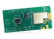
Infineon Technologies CYBLE-212006-EVAL EZ-BLE PROC 평가 보드
EZ-BLE PRoC 모듈(CYBLE-212006-01)에서 애플리케이션을 평가 및 개발할 수 있습니다.
Block Diagram

게시일: 2016-04-25
| 갱신일: 2025-08-19