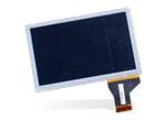
디스플레이 개발 툴 10.4 IN Optical Bond DEV KIT
TKL-104XOB-18054-A
KYOCERA Display
1:
₩1,074,047.2
5 재고 상태
Mouser 부품 번호 805-TKL104XOB18054A
KYOCERA Display
디스플레이 개발 툴 10.4 IN Optical Bond DEV KIT
5 재고 상태
구매
최소: 1 배수: 1
세부 정보
Development Kits
KDA104OB-18054S-A
LVDS
디스플레이 개발 툴 7 IN Optical Bond DEV KIT
TKL-070WOB-18052-A
KYOCERA Display
1:
₩741,790.4
15 재고 상태
Mouser 부품 번호 805-TKL070WOB18052A
KYOCERA Display
디스플레이 개발 툴 7 IN Optical Bond DEV KIT
15 재고 상태
구매
최소: 1 배수: 1
세부 정보
Development Kits
KDA-070OB-18052-A
LVDS
디스플레이 개발 툴 Optically bonded TFT LCD Display Development Kit includes the display, graphic board, OSD board, interface cable, backlight cable if needed, VGA and DVI cables and power kit.
TKL-070WOB-18053-A
KYOCERA Display
30:
₩458,523.2
비재고 리드 타임 28 주
Mouser 부품 번호 805-TKL070WOB18053A
KYOCERA Display
디스플레이 개발 툴 Optically bonded TFT LCD Display Development Kit includes the display, graphic board, OSD board, interface cable, backlight cable if needed, VGA and DVI cables and power kit.
비재고 리드 타임 28 주
구매
최소: 30 배수: 30
세부 정보
Development Kits
LVDS
디스플레이 개발 툴 Optically bonded TFT LCD Display Development Kit includes the display, graphic board, OSD board, interface cable, backlight cable if needed, VGA and DVI cables and power kit.
TKL-084SOB-18051-A
KYOCERA Display
20:
₩958,861.6
비재고 리드 타임 28 주
Mouser 부품 번호 805-TKL084SOB18051A
KYOCERA Display
디스플레이 개발 툴 Optically bonded TFT LCD Display Development Kit includes the display, graphic board, OSD board, interface cable, backlight cable if needed, VGA and DVI cables and power kit.
비재고 리드 타임 28 주
구매
최소: 20 배수: 20
세부 정보
Development Kits
KDA084OB-18051S-A
LVDS
디스플레이 개발 툴 Optically bonded TFT LCD Display Development Kit includes the display, graphic board, OSD board, interface cable, backlight cable if needed, VGA and DVI cables and power kit.
TKL-104SOB-18078-A
KYOCERA Display
20:
₩982,330.4
비재고 리드 타임 28 주
Mouser 부품 번호 805-TKL104SOB18078A
KYOCERA Display
디스플레이 개발 툴 Optically bonded TFT LCD Display Development Kit includes the display, graphic board, OSD board, interface cable, backlight cable if needed, VGA and DVI cables and power kit.
비재고 리드 타임 28 주
구매
최소: 20 배수: 20
세부 정보
Development Kits
KDA104OB-18078S-A
LVDS
디스플레이 개발 툴 12.1 IN Optical Bond DEV KIT
TKL-121WOB-18055-A
KYOCERA Display
10:
₩1,472,332.8
비재고 리드 타임 28 주
Mouser 부품 번호 805-TKL121WOB18055A
KYOCERA Display
디스플레이 개발 툴 12.1 IN Optical Bond DEV KIT
비재고 리드 타임 28 주
구매
최소: 10 배수: 10
세부 정보
Development Kits
KDA-121OB-18055S-A
LVDS
디스플레이 개발 툴 Optically bonded TFT LCD Display Development Kit includes the display, graphic board, OSD board, interface cable, backlight cable if needed, VGA and DVI cables and power kit.
TKL-121WOB-18079-A
KYOCERA Display
10:
₩1,444,501.6
비재고 리드 타임 28 주
Mouser 부품 번호 805-TKL121WOB18079A
KYOCERA Display
디스플레이 개발 툴 Optically bonded TFT LCD Display Development Kit includes the display, graphic board, OSD board, interface cable, backlight cable if needed, VGA and DVI cables and power kit.
비재고 리드 타임 28 주
구매
최소: 10 배수: 10
세부 정보
Development Kits
KDA-121OB-18079S-A
LVDS
디스플레이 개발 툴 Optically bonded TFT LCD Display Development Kit includes the display, graphic board, OSD board, interface cable, backlight cable if needed, VGA and DVI cables and power kit.
TKL-121XOB-18056-A
KYOCERA Display
10:
₩1,139,194.4
비재고 리드 타임 28 주
Mouser 부품 번호 805-TKL121XOB18056A
KYOCERA Display
디스플레이 개발 툴 Optically bonded TFT LCD Display Development Kit includes the display, graphic board, OSD board, interface cable, backlight cable if needed, VGA and DVI cables and power kit.
비재고 리드 타임 28 주
구매
최소: 10 배수: 10
세부 정보
Development Kits
KDA121OB-18056S-A
LVDS


 대한민국
대한민국