High Power Factor Flyback with Constant-Current Output for LED Lighting Applications
By Michael Weirich, The Global Power Resource
SM Center (GPRC) Europe
Featured Suppliers
Resources
Abstract — This article explains the principles of AC/DC converters in flyback topology having a high power factor input and a constant current output. The most commonly used mode of operation for this purpose is boundary conduction mode (BCM). The basics of this mode are developed and its drawbacks are made clear. A simple method for improving power factor is introduced and explained in detail. Operating in DCM mode improves power factor and THD while reducing the peak drain voltage. A quick design example is given and the special issues of driving high power LEDs are explained.
Introduction
Due to their long lifetime and excellent efficacy, high-power LEDs are increasingly used in general lighting applications. Two things are important when driving LEDs: they must be operated with constant current and the ballast must have a high power factor. While international standards dictate power factor correction mandatory for input powers above 25W, the new Energy-Star directive for solid-state lighting requires a power factor greater than 0.9 for power levels above 3W.
While it is possible to achieve this by passive power factor correction (PFC), it is desirable to have a costeffective solution that can achieve even better performance with low weight and small form factor. A flyback converter with low harmonic content input current is one possible solution.
High Power Factor Flyback: Basics of Operation
The basic idea behind the high power factor (PF) flyback is to control it using a boundary conduction mode (BCM) PFC controller like the FAN7527B. The FAN7527B forces the peak drain current to follow the shape of the input voltage similar to a PFC preregulator in boost topology but with some differences in operation.
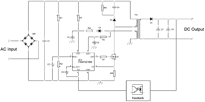
First, the bulk capacitor after the rectifier is removed which is the primary reason for poor power factor of the switch-mode power supply (SMPS). This is because it only allows input current flow when the input voltage is higher than the voltage of the bulk capacitor which is essentially constant. Thus, the input current of a SMPS with a bulk capacitor consists of short and high peaks having high harmonic content and higher RMS and peak values than a sinusoidal current would have at same output power. In contrast, the value of C1 in the simplified schematic (Fig. 1) is only a few hundreds of a nF and this cap acts as a high frequency filter only. Obviously, the flyback following this input stage is not supplied by a DC voltage but by half-waves with double the line frequency.

Fig. 1: Simplified schematic of high-power flyback operating in BCM.
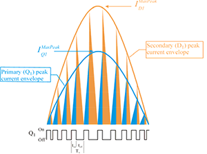
The basic operation of the flyback is as follows: When MOSFET Q1 is turned on, the current in the primary side of the transformer increases linearly. The current through Q1 is sensed with R8 and the corresponding voltage is fed to the sense pin ‘CS’ of the controller. An internal comparator turns the MOSFET off as soon as the sense pin reaches a level that is determined by the voltage at the pin ‘MULT’ and the output of the error amplifier. To allow a good power factor, the error amplifier output must be nearly constant during one half–cycle of the input voltage. Thus, the shape of the peak drain current is determined by the voltage at the ‘MULT’ input, which is the rectified and scaled down input voltage. Consequently, if the input voltage is sinusoidal, the envelope of the primary side peak drain current is sinusoidal as well.

Fig. 2: Timing and currents in BCM flyback.
Since both the rate of change of the inductor current and the peak inductor current are proportional to the instantaneous input voltage, the on-time is constant over the complete half-cycle.
When the MOSFET is turned off, the input current instantly drops to zero, unlike the boost converter where it goes down linearly. As in any flyback the secondary side diode now conducts and the energy stored in the magnetic field is transferred to the output. The diode current decreases linearly, starting from a value that is n times higher than the primary side peak, with n being the transformer turns primary to secondary turns ratio. The diode current drops at a constant rate while the peak value is proportional to the momentary input voltage. This leads to a variable time until the current falls to zero and the next switching cycle is initiated. Together with the constant on-time, the variable off-time results in a variable switching frequency.
To determine the actual shape of the input current, the average value of the transformer current has to be determined; in the real application, the EMI filter will do that for you. For this purpose, the momentary switching frequency and duty cycle are needed.
First, the on-time of Q1 is calculated (Θ is defined as 2·Π·f
L·t with f
L being the line frequency):
This formula confirms that tOn is constant over a half-cycle. The off-time is given by:
As expected, the off-time varies over the half-cycle. Together, equations (1) and (2) give the switching period, TS:
One important design parameter for flyback topology is the reflected voltage (1) VR = n · (VOut + VFwdD1) , which is the voltage that occurs across the primary side of the transformer while the secondary diode is conducting. A higher VR value increases the voltage stress on the MOSFET drain. Because of this, there is the general tendency to keep VR small. The switching frequency is derived from Equation (3), resulting in a simpler formula:
From this formula, the minimum switching frequency always occurs at the line voltage maximum, while the maximum frequency is reached at the line zero crossing. One important design parameter is missing: duty-cycle d, given by the equation:
and varies over the line cycle in the same way the switching frequency does.
The next issue is to determine whether the input current will be sinusoidal (as was originally intended). Only the expression for the variation of the peak MOSFET current with time, or better to say with phase angle, has to be determined. Bearing in mind that this peak value is forced to follow the shape of the input voltage (Fig. 2), this equation can be expressed as follows:
The current averaged over one switching cycle is then given by the area of the triangular drain current times the momentary duty cycle:
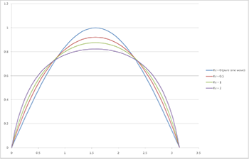
The result of (7) is quite disappointing since the denominator makes the current shape clearly nonsinusoidal, unless the ratio RVR=VPeak In/VR is made very small. It is clearly visible from Fig. 3 that for RV > 1, the current is not sinusoidal.

Fig. 3: Shape of the input current of BCM flyback with RVR as an parameter.
Note that the reflected voltage, VR, adds to the input voltage during the off-time of the MOSFET. Making the ratio small, such as 0.1, would result in a drain voltage which is more than eleven times the input voltage. Such a high reflected voltage is impossible to handle even if the input voltage is only 110VRMS. Feasible values for RVR are in the range of 1 for US and 2 to 3 for European input voltage. Harmonic analysis of the input current shape shows that it is difficult to get a THD lower than 10%, mandatory for lighting equipment above 25W, with a RVR of 2. Hence, the described application is more suited for US input voltages. For European applications, an 800V or even an 1000V MOSFET must be used to comply with the regulations for lighting equipment. Nevertheless, the power factor itself is still in the range of 0.95 when RVR is 2 and the BCM flyback method for PFC is usable for many applications that need a relatively high PF but not a low THD.
A careful review of the equations above lead to the following conclusions:
- The input voltage as a reference for the MOSFET peak drain current is not needed. If the on-time is made constant over one half-cycle, the peak drain current will follow the input voltage.
- The main reason for the non-ideal shape of the input current is the variable frequency or rather the variable duty-cycle. With the identical drain current shape, if the duty-cycle were kept constant over a half-cycle, the input current would be sinusoidal.
Obviously these two things can be accomplished with a “traditional” PWM controller. This implementation is most easy if a voltage mode (VM) controller is used. If the feedback loop is slow enough, the duty cycle will be constant i.e. the desired constant on-time is achieved. Unfortunately it is difficult to find a state of the art voltage mode controller for offline applications on the market since current mode devices have so many advantages for standard off-line applications. A possible choice is the KA7552A or KA7553A which differ only in the maximum dutycycle.
If a current mode (CM) controller is used, the peak current has to be set to be proportional to the input voltage as implemented in current mode PFC controllers. But these devices are all designed for BCM and must be driven by an external oscillator to operate with constant fS. Hence, the voltage mode PWM controller seems to be a smart choice.
As will be shown later, it is possible to turn the BCM controllers FAN7527 (CM), FAN7529/30 (VM), FAN6961 (VM), and similar into constant frequency controllers with a few inexpensive external components.
 Dr. Michael Weirich is the head of the Global Power Resource Center Europe. After finishing his Ph.D. thesis in solid state physics at the ‘Universität des Saarlandes’ in Germany, he started as a designer for analog and power electronics at the Siems & Becker GMBH, Bonn. Before he joined Fairchild in 2003, he worked several years as engineering manager in the design of fluorescent lamp ballasts at the OSRAM GmbH, Munich.